
| Tweet |

Custom Search
|
|

|
||
 TM 9-8000
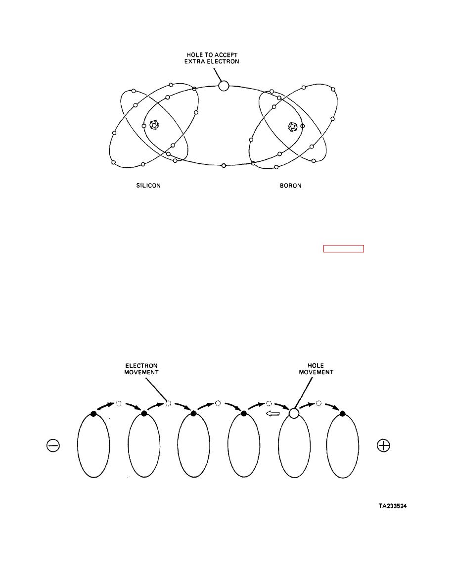
Figure 11-6. Boron-Doped Silicon.
negative side of the circuit and the positive side of the
Without the presence of holes at the junction, the
circuit is connected to the P-material.
In this
electrons cannot cross it.
configuration, which is known as forward bias, the diode
is a good conductor. This is because the positively
11-7.
Zener Diodes (Fig. 11-9). The diode, as
charged holes in the P-type material move toward the
described in paragraph 11-6, is a semiconductor device
junction with the negatively charged N-material so that
that allows current to flow only in one direction. A zener
electrons may cross the junction and fill these holes
diode, however, is a special type that allows reverse
using them to move across the P-material. If the
current to flow as long as the voltage is above a value
connections to the diode are reversed, current flow will
that is built into the device when it is manufactured. As
be blocked. This configuration is known as reverse bias.
an example, a certain zener diode may not conduct
When the diode is connected backwards, the positively
current if the reverse bias voltage is below 6 volts. As
charged holes are attracted away from the junction to the
the voltage increases to 6 volts or more, the diode
negative terminal and the free electrons in the N-material
suddenly will begin to conduct reverse bias current. This
are attracted away from the junction to the positive
device is used in control circuits such as voltage
terminal.
regulators.
Figure 11-7. Hole Movement Theory.
11-6
|
||
|
||


