
| Tweet |

Custom Search
|
|

|
||
 TM 9-8000
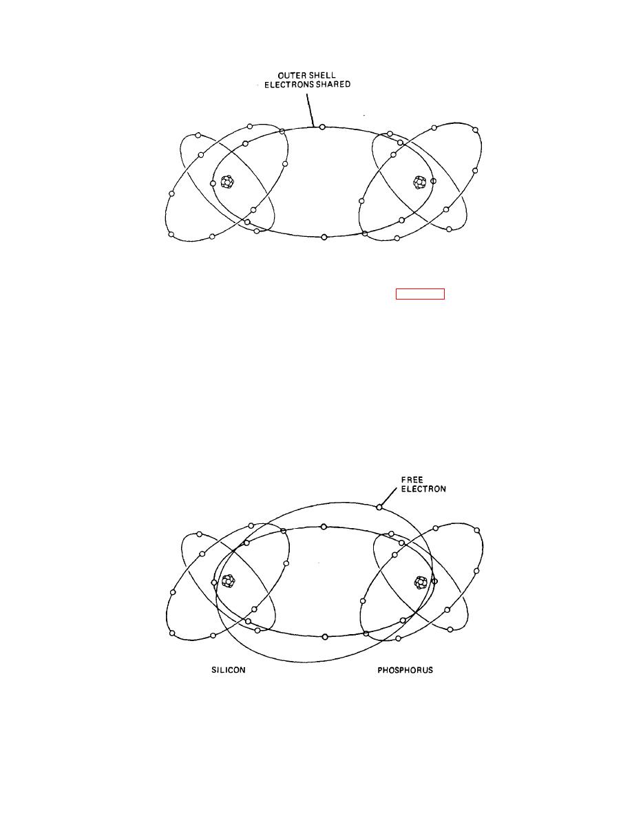
Figure 11-4. Covalent Bonding OF Silicon.
electrons, the same as the current flow through a natural
11-6. Diodes(Fig. 11-8).
conductor such as copper. When a current source of
sufficient voltage is connected across a P-type material,
a. Purpose. A diode is a device that will allow
an electric current will also flow through it, but any
current to pass through itself in only one direction. A
current flow in a P-type semiconductor is looked upon as
diode can be thought of as an electrical checkvalve.
the movement of positively charged holes. The holes
appear to move toward the negative terminal as the
b. Construction. A diode is made by joining N-type
electrons enter the material at the negative terminal, fill
material and P-type material together. The negative
the holes, and then move from hole to hole toward the
electrical terminal is located at the N-type material and
positive terminal. As is the case with N-type semi-
the positive terminal is located on the P-type material.
conductors, the movement of electrons through P-type
semiconductors toward the positive terminal is motivated
c. Operation. When a diode is placed in a circuit,
by the natural attraction of unlike charges.
the N-material is connected to the
TA233523
Figure 11-5. Phosphorus-Doped Silicon.
11-5
|
||
|
||


